Fermi surface
In condensed matter physics, the Fermi surface is an abstract boundary in reciprocal space useful for predicting the thermal, electrical, magnetic, and optical properties of metals, semimetals, and doped semiconductors. The shape of the Fermi surface is derived from the periodicity and symmetry of the crystalline lattice and from the occupation of electronic energy bands. The existence of a Fermi surface is a direct consequence of the Pauli exclusion principle, which allows a maximum of one electron per quantum state.[1][2] [3][4]
Theory
Consider a spinless ideal Fermi gas of particles. According to Fermi–Dirac statistics, the mean occupation number of a state with energy is given by[6]
where,
- is the mean occupation number of the state
- is the kinetic energy of the state
- is the internal chemical potential (at zero temperature, this is the maximum kinetic energy the particle can have, i.e. Fermi energy )
- is the absolute temperature
- is the Boltzmann constant
Suppose we consider the limit . Then we have,
By the Pauli exclusion principle, no two fermions can be in the same state. Therefore, in the state of lowest energy, the particles fill up all energy levels below , which is equivalent to saying that is the energy level below which there are exactly states.
In momentum space, these particles fill up a sphere of radius , the surface of which is called the Fermi surface.[7]
The linear response of a metal to an electric, magnetic or thermal gradient is determined by the shape of the Fermi surface, because currents are due to changes in the occupancy of states near the Fermi energy. Free-electron Fermi surfaces are spheres of radius
determined by the valence electron concentration where is the reduced Planck's constant. A material whose Fermi level falls in a gap between bands is an insulator or semiconductor depending on the size of the bandgap. When a material's Fermi level falls in a bandgap, there is no Fermi surface.

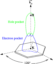
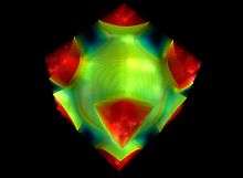
Materials with complex crystal structures can have quite intricate Fermi surfaces. The figure illustrates the anisotropic Fermi surface of graphite, which has both electron and hole pockets in its Fermi surface due to multiple bands crossing the Fermi energy along the direction. Often in a metal the Fermi surface radius is larger than the size of the first Brillouin zone which results in a portion of the Fermi surface lying in the second (or higher) zones. As with the band structure itself, the Fermi surface can be displayed in an extended-zone scheme where is allowed to have arbitrarily large values or a reduced-zone scheme where wavevectors are shown modulo (in the 1-dimensional case) where a is the lattice constant. In the three-dimensional case the reduced zone scheme means that from any wavevector there is an appropriate number of reciprocal lattice vectors subtracted that the new now is closer to the origin in -space than to any . Solids with a large density of states at the Fermi level become unstable at low temperatures and tend to form ground states where the condensation energy comes from opening a gap at the Fermi surface. Examples of such ground states are superconductors, ferromagnets, Jahn–Teller distortions and spin density waves.
The state occupancy of fermions like electrons is governed by Fermi–Dirac statistics so at finite temperatures the Fermi surface is accordingly broadened. In principle all fermion energy level populations are bound by a Fermi surface although the term is not generally used outside of condensed-matter physics.
Experimental determination
Electronic Fermi surfaces have been measured through observation of the oscillation of transport properties in magnetic fields , for example the de Haas–van Alphen effect (dHvA) and the Shubnikov–de Haas effect (SdH). The former is an oscillation in magnetic susceptibility and the latter in resistivity. The oscillations are periodic versus and occur because of the quantization of energy levels in the plane perpendicular to a magnetic field, a phenomenon first predicted by Lev Landau. The new states are called Landau levels and are separated by an energy where is called the cyclotron frequency, is the electronic charge, is the electron effective mass and is the speed of light. In a famous result, Lars Onsager proved that the period of oscillation is related to the cross-section of the Fermi surface (typically given in ) perpendicular to the magnetic field direction by the equation . Thus the determination of the periods of oscillation for various applied field directions allows mapping of the Fermi surface.
Observation of the dHvA and SdH oscillations requires magnetic fields large enough that the circumference of the cyclotron orbit is smaller than a mean free path. Therefore, dHvA and SdH experiments are usually performed at high-field facilities like the High Field Magnet Laboratory in Netherlands, Grenoble High Magnetic Field Laboratory in France, the Tsukuba Magnet Laboratory in Japan or the National High Magnetic Field Laboratory in the United States.

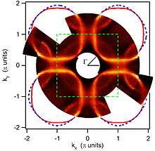
The most direct experimental technique to resolve the electronic structure of crystals in the momentum-energy space (see reciprocal lattice), and, consequently, the Fermi surface, is the angle resolved photoemission spectroscopy (ARPES). An example of the Fermi surface of superconducting cuprates measured by ARPES is shown in the figure.
With positron annihilation it is also possible to determine the Fermi surface as the annihilation process conserves the momentum of the initial particle. Since a positron in a solid will thermalize prior to annihilation, the annihilation radiation carries the information about the electron momentum. The corresponding experimental technique is called angular correlation of electron positron annihilation radiation (ACAR) as it measures the angular deviation from 180 degree of both annihilation quanta. In this way it is possible to probe the electron momentum density of a solid and determine the Fermi surface. Furthermore, using spin polarized positrons, the momentum distribution for the two spin states in magnetized materials can be obtained. ACAR has many advantages and disadvantages compared to other experimental techniques: It does not rely on UHV conditions, cryogenic temperatures, high magnetic fields or fully ordered alloys. However, ACAR needs samples with a low vacancy concentration as they act as effective traps for positrons. In this way, the first determination of a smeared Fermi surface in a 30% alloy was obtained in 1978.
See also
References
- ↑ N. Ashcroft and N.D. Mermin, Solid-State Physics, ISBN 0-03-083993-9
- ↑ W.A. Harrison, Electronic Structure and the Properties of Solids, ISBN 0-486-66021-4
- ↑ VRML Fermi Surface Database
- ↑ J. M. Ziman, Electrons in Metals: A short Guide to the Fermi Surface (Taylor & Francis, London, 1963), ASIN B0007JLSWS.
- ↑ Weber, J. A.; Böni, P.; Ceeh, H.; Leitner, M.; Hugenschmidt, Ch (2013-01-01). "First 2D-ACAR Measurements on Cu with the new Spectrometer at TUM". Journal of Physics: Conference Series. 443 (1): 012092. doi:10.1088/1742-6596/443/1/012092. ISSN 1742-6596.
- ↑ (Reif 1965, p. 341)
- ↑ K. Huang, Statistical Mechanics (2000), p. 244
External links
- Experimental Fermi surfaces of some superconducting cuprates and strontium ruthenates in "Angle-resolved photoemission spectroscopy of the cuprate superconductors (Review Article)" (2002)
- Experimental Fermi surfaces of some cuprates, transition metal dichalcogenides, ruthenates, and iron based superconductors in "ARPES experiment in fermiology of quasi-2D metals (Review Article)" (2014)
- Dugdale, S. B. (2016-01-01). "Life on the edge: a beginner's guide to the Fermi surface". Physica Scripta. 91 (5): 053009. doi:10.1088/0031-8949/91/5/053009. ISSN 1402-4896.
