Milbeaut

The Socionext Milbeaut image/video processors are media processors in multi-processor system on a chip architecture.[1][2] Started by Fujitsu with the M-1 Series in 2000 each generation (2013: 7th) has several variants regarding included modules and processor-cores, built for mobile phones, digital compact cameras, MILCs and DSLRs like Leica M and Leica S2,[3] Nikon DSLRs (see Nikon EXPEED), some Pentax K mount[4] cameras and for the Sigma True-II processor.[5]
Technology
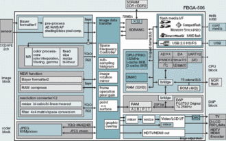
Multiple FR-V processor cores, with even each single processor-core able to compute many instructions/operations in parallel are used for image- and video-processing. Storage- and display-interfaces and other modules are added and a digital signal processor (DSP) increases the number of simultaneous computations.
An on-chip 32-bit Fujitsu FR microcontroller (6th generation in 2011 introduced the dual-core ARM architecture) initiates and controls the operation and data transfers of all processors, modules and interfaces and can be seen as the main control unit of the camera. The Milbeaut is also used as an application-specific integrated circuit (ASIC) or application-specific standard product (ASSP).
The 7th generation uses a 55 nm low-power process (SuVolta) and ARM Cortex-A5 microcontroller.[6]
References
- ↑ Fujitsu: Milbeaut Imaging Processors
- ↑ Fujitsu: Image processing system for digital cameras: Milbeaut M-4
- ↑ Fujitsu Microelectronics-Leica's Image Processing System Solution For High-End DSLR
- ↑ Pentax hack: Hardware info
- ↑ Sigmauser: TRUE Strengths. Written by Stuart Dennison
- ↑ "Fujitsu Releases New Milbeaut® Image Processor" (Press release). Fujitsu. September 4, 2013. Retrieved March 30, 2014.
