Optical modulators using semiconductor nano-structures
An optical modulator is an optical device which is used to modulate a beam of light with a perturbation device. It is a kind of transmitter to convert information to optical binary signal through optical fiber (optical waveguide) or transmission medium of optical frequency in fiber optic communication. There are several methods to manipulate this device depending on the parameter of a light beam like amplitude modulator (majority), phase modulator, polarization modulator etc. The easiest way to obtain modulation is modulation of intensity of a light by the current driving the light source (laser diode). This sort of modulation is called direct modulation, as opposed to the external modulation performed by a light modulator. For this reason, light modulators are called external light modulators. According to manipulation of the properties of material modulators are divided into two groups, absorptive modulators (absorption coefficient) and refractive modulators (refractive index of the material). Absorption coefficient can be manipulated by Franz-Keldysh effect, Quantum-Confined Stark Effect, excitonic absorption, or changes of free carrier concentration. Usually, if several such effects appear together, the modulator is called electro-absorptive modulator. Refractive modulators most often make use of electro-optic effect (amplitude & phase modulation), other modulators are made with acousto-optic effect, magneto-optic effect such as Faraday and Cotton-Mouton effects. The other case of modulators is spatial light modulator (SLM) which is modified two dimensional distribution of amplitude & phase of an optical wave.
Optical modulators can be implemented using Semiconductor Nano-structures to increase the performance like high operation, high stability, high speed response, and highly compact system. Highly compact electro-optical modulators have been demonstrated in compound semiconductors.[1] However, in silicon photonics, electro-optical modulation has been demonstrated only in large structures, and is therefore inappropriate for effective on-chip integration. Electro-optical control of light on silicon is challenging owing to its weak electro-optical properties. The large dimensions of previously demonstrated structures were necessary to achieve a significant modulation of the transmission in spite of the small change of refractive index of silicon. Liu et al. have recently demonstrated a high-speed silicon optical modulator based on a metal–oxide–semiconductor (MOS) configuration.[2] Their work showed a high-speed optical active device on silicon—a critical milestone towards optoelectronic integration on silicon.
Electro-optic modulator of nano-structures
An electro-optic modulator is a device which can be used for controlling the power, phase or polarization of a laser beam with an electrical control signal. It typically contains one or two Pockels cells, and possibly additional optical elements such as polarizers. The principle of operation is based on the linear electro-optic effect (the Pockels effect, the modification of the refractive index of a nonlinear crystal by an electric field in proportion to the field strength).
The crystal which is covered by electrode may be considered to be a voltage-variable wave-plate. When a voltage is applied, the retardation of laser polarization of the light would be changed while a beam passes through an ADP crystal. This variation in polarization results in intensity modulation downstream from the output polarizer. The output polarizer converts the phase shift into an amplitude modulation.
Micrometre-scale silicon electro-optic modulator[3]
This device was fabricated a shape of the p-i-n ring resonator on a silicon-on-insulator substrate with a 3-mm-thick buried oxide layer. Both the waveguide coupling to the ring and that forming the ring have awidth of 450 nm and a height of 250 nm. The diameter of the ring is 12 mm, and the spacing between the ring and the straight waveguide is 200 nm.
Acousto-optic modulator of nano-structures
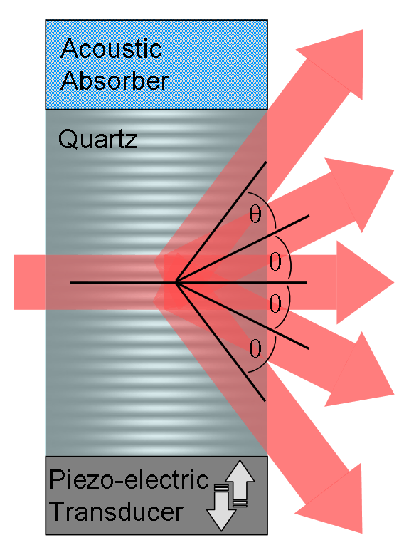
Acousto-optic modulators are used to vary and control laser beam intensity. A Bragg configuration gives a single first order output beam, whose intensity is directly linked to the power of RF control signal. The rise time of the modulator is simply deduced by the necessary time for the acoustic wave to travel through the laser beam. For highest speeds the laser beam will be focused down, forming a beam waist as it passes through the modulator.
In an AOM a laser beam is caused to interact with a high frequency ultrasonic sound wave inside an optically polished block of crystal or glass (the interaction medium). By carefully orientating the laser with respect to the sound waves the beam can be made to reflect off the acoustic wave-fronts (Bragg diffraction). Therefore, when the sound field is present the beam is deflected and when it is absent the beam passes through undeviated. By switching the sound field on and off very rapidly the deflected beam appears and disappears in response (digital modulation). By varying the amplitude of the acoustic waves the intensity of the deflected beam can similarly be modulated (analogue modulation).

Acoustic solitons in semiconductor nanostructures[4]
Acoustic solitons strongly influence the electron states in a semiconductor nanostructure. The amplitude of soliton pulses is so high that the electron states in a quantum well make temporal excursions in energy up to 10 meV. The subpicosecond duration of the solitons is less than the coherence time of the optical transition between the electron states and a frequency modulation of emitted light during the coherence time (chirping effect) is observed. This system is for an ultrafast control of electron states in semiconductor nanostructures.
Magneto-optic modulator of nano-structures
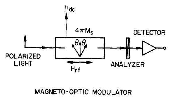
A dc magnetic field Hdc is applied perpendicular to the light propagation direction to produce a single domain, transverse directed 4~Ms. The rf modulation field Hrf, applied by means of a coil along the light propagation direction, wobbles 4~Ms through an angle of @ and produces a time varying magnetization component in the longitudinal direction. This component then produces an ac variation in the plane of polarization via the longitudinal Faraday effect. Conversion to amplitude modulation is accomplished by the indicated analyzer.

Wideband magneto-optic modulation in a bismuth-substituted yttrium iron garnet waveguide[5]
The current transient creates a time-varying magnetic field that has a component along the direction of optical propagation. This component (underneath the microstrip line) acts to tip the magnetization, M, along the propagation direction of the optical beam. A static in-plane magnetic field, by, is applied perpendicular to the light propagation direction, thus ensuring the return of M to its initial orientation after the passage of the current transient. Depending on the component of the magnetization along the z-direction, Mz, the optical beam experiences a rotation of its polarization due to the Faraday effect. The polarization modulation is converted into an intensity modulation via a polarization analyzer, which is detected by a high-speed photodiode.
Other semiconductor nanostructures of optical modulator
MODULATION OF THz RADIATION BY SEMICONDUCTOR NANOSTRUCTURES[6]
As a result of increased demand for bandwidth, wireless short-range communication systems are expected to extend into the THz frequency range. Therefore, the fundamental interactions between THz radiation and semiconductors are receiving increasing attention. This new quantum structure is based on the well-established technology for producing high electron mobility transistors where an electron gas is confined at a GaAs/AlxGa1 xAs interface. The electron density at the hetero-interface can be controlled by the application of an external gate voltage, which in turn will alter the transmission/reflection characteristics of the device to an incident THz beam.
Applications and Commercial products
Electro-optic modulator
- from THORLABS
40 Gbit/s Phase Modulator The 40 Gbit/s Phase Modulator is a high performance, low drive voltage External Optical Modulator designed for customers developing next generation 40G transmission systems. The increased bandwidth allows for chirp control in high-speed data communications.
Applications ; Chirp Control for High-Speed Communications (SONET OC-768 Interfaces, SDH STM-256 Interfaces), Coherent communications, C & L Band Operation, Optical Sensing, All-optical frequency shifting.
- from Mach-40
Acousto-optic modulator of nano-structures
Applications ; acousto-optic modulators include laser printing, video disk recording, laser projection systems.
- from ELECTRO-OPTICAL PRODUCTS CORPORATION
References
- ↑ Sadagopan, T., Choi, S. J., Dapkus, P. D. & Bond, A. E. Digest of the LEOS Summer Topical Meetings MC2–-3 (IEEE, Piscataway, New Jersey (2004)
- ↑ Liu, A. et al. Nature 427, 615–618 (2004)
- ↑ Nature 435, 325–327 (19 May 2005)
- ↑ Journal of Physics: Conference Series 92 (PHONONS 2007)
- ↑ Optics Communications Volume 220, Issues 4–6
- ↑ MICROWAVE AND OPTICAL TECHNOLOGY LETTERS / Vol. 35, No. 5, December 5, 2002